|
This research combines the knowledge of
nano-optics and nano-fabrication for the development of optical
antennas. In a three-step approach, our structures are first modeled,
designed and simulated using Microwave Studio, Finite Difference Time
Domain (FDTD), and Discrete Dipole Approximation (DDA). Extensive
studies of field distribution, extinction efficiency and their
dependence on geometry are carried out prior to physical design.
The nanostructures are fabricated using electron-beam lithography and a
novel nanofabrication technique developed by our group called
Solid-state superionic stamping (Hsu et al., Nano Lett. 7 (2), 446). We
focus on improving the capabilities of current fabrication capabilities
beyond 20 nm feature size with added advantages of low cost, high
throughput, ambient conditions, and large area patterning.
Antenna
characterization involves several different approaches
• Optical measurements for extinction and scattering
analysis
• High-resolution cathodoluminescence imaging and
spectroscopy for analyzing various antenna modes with sub-20 nm
resolution
• Second-harmonic generation and metal-enhanced
fluorescence utilizing the high fields in bowtie antenna gaps
Additionally, thin films of noble metals are explored to
reduce scattering losses in plasmonic devices due to film roughness. In
these studies, a different approach based on buffer layer of various
materials, e.g., Ge, MgO, NiO is first grown below the metal film that
helps improve the growth process (Logeeswaran, Nano Lett., 2009).We apply our understanding of plasmonics and antenna theory to optical
wavelengths and explore ways to utilize these sub-wavelength resonant
structures for molecular imaging, nanolithography, solar cell efficiency
improvement, data storage and optical communication.
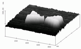
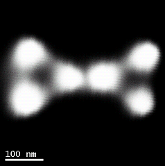
Figure. AFM image of a bowtie
antenna (left) and a high-resolution cathodoluminescence image (right)
showing the out-of-plane plasmonic mode of the nanostructures. |