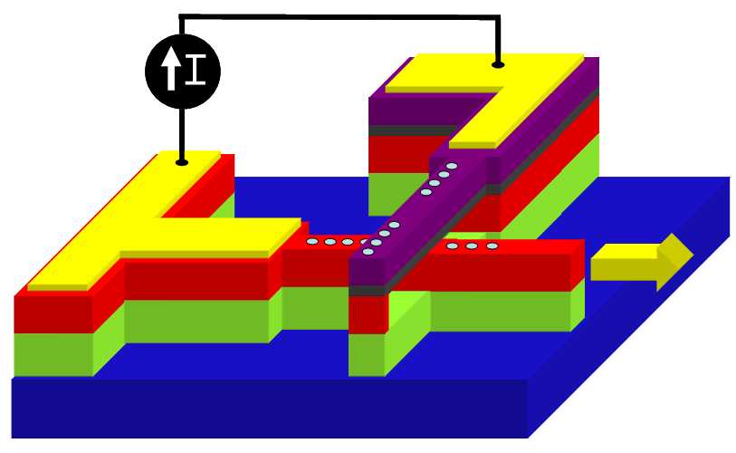
Figure 1) Schematic of the nanocavity photonic crystal laser
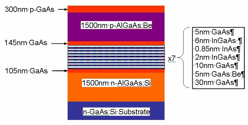
Figure 2) Structure of a semiconductor laser with an active region consisting of seven layers of InAs quantum dots embedded within InGaAs quantum wells and GaAs barriers.
The goal of this work is to design and fabricate semiconductor lasers with novel quantum dot layers
in the active region with the goal of incorporating these active regions within nanocavity photonic crystal
lasers (Figure 1). Quantum-dot (QD) heterostructure lasers are a type of semiconductor laser that utilize
quantum dots as the active media within the light-emitting region. Quantum dots are semiconductor
nanocrystals of narrow band-gap material that are embedded in a wider band-gap material. The use of
molecular beam epitaxy for the growth of highly lattice-mismatched III-V semiconductor materials has
made the self-assembly of these structures possible. Due to the strong three-dimensional carrier confinement,
devices that employ quantum dots have unique capabilities that are otherwise practically unachievable
with bulk semiconductors, or even with quantum well structures.
One of the significant benefits of exploiting quantum effects in QD semiconductor lasers is to
achieve lower threshold current densities. A reduction in the threshold current density
is a direct result of the reduction in the translational degrees of freedom of the charge
carriers (electrons and holes) thereby leading to an increase in the density of states of
the charge carriers near the band edges. Another important benefit is that the threshold
current density in QD lasers is unaffected by temperatures up to about 300K since the
carriers can only be thermally excited to a very limited number of these well-spaced energy
levels within the quantum dots.
To evaluate the use of quantum dots within the active region of a photonic crystal laser, a separate confinement
heterostructure laser with 7 layers of quantum dots is being fabricated. A SCH laser provides
electrical confinement via the energy band structure while optical confinement is achieved by means of
ridge waveguides and index contrast. The semiconductor laser consists of epitaxially-grown layers of
both doped and undoped semiconductor on n-GaAs substrate (Figure 2).
The photonic crystal laser design (schematically shown in Figure 1) incorporates one-dimensional
(1-D) photonic crystals patterned on two crossing waveguides. The nanocavity, located at the two waveguide’s
intersection, creates a high-Q optical resonator with the 1-D photonic crystals acting as highly
reflective mirrors. By removing some of the holes in one of the photonic crystals, one can control
the direction of the emitted light. The top GaAs-based waveguide is doped p-type, while the
bottom, InGaAlP-based waveguide, is doped n-type, so that a p-n diode exists only in the area
where the waveguides overlap. The top GaAs waveguide contains a quantum dots-in-a-well structure,
which serves as the active material for the laser.
The quantum dot and nanocavity photonic crystal lasers will be characterizated both in the CW and pulsed
mode of operation at a variety of temperatures. The use of interchangeable InGaAs and PbS detectors will allow
for a good sensitivity for emission wavelengths less than 2.5microns.
